P-type semiconductors are created by doping silicon with elements that have fewer valence electrons, introducing positive charge carriers known as holes. N-type semiconductors result from doping silicon with elements that have extra valence electrons, providing an abundance of free electrons as charge carriers. The interaction between these two types forms the basis of p-n junctions, essential for controlling current flow in diodes and transistors.
Table of Comparison
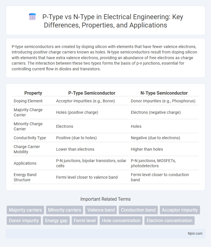
| Property | P-Type Semiconductor | N-Type Semiconductor |
|---|---|---|
| Doping Element | Acceptor impurities (e.g., Boron) | Donor impurities (e.g., Phosphorus) |
| Majority Charge Carrier | Holes (positive charge) | Electrons (negative charge) |
| Minority Charge Carrier | Electrons | Holes |
| Conductivity Type | Positive (due to holes) | Negative (due to electrons) |
| Charge Carrier Mobility | Lower than electrons | Higher than holes |
| Applications | P-N junctions, bipolar transistors, solar cells | P-N junctions, MOSFETs, photodetectors |
| Energy Band Structure | Fermi level closer to valence band | Fermi level closer to conduction band |
Introduction to P-Type and N-Type Semiconductors
P-type semiconductors are created by doping intrinsic silicon with elements such as boron that introduce electron "holes," enabling positive charge carriers. N-type semiconductors result from doping silicon with elements like phosphorus, which add extra electrons acting as negative charge carriers. These two types form the basis of semiconductor devices by controlling electric current through charge carrier manipulation.
Formation and Doping Methods
P-type semiconductors are formed by doping intrinsic silicon with trivalent elements such as boron or gallium, creating holes as majority carriers by accepting electrons. N-type semiconductors result from doping silicon with pentavalent elements like phosphorus or arsenic, introducing extra electrons that act as majority carriers. These doping methods adjust the semiconductor's electrical conductivity by altering carrier concentration through precise control of impurity atom incorporation during crystal growth or diffusion processes.
Charge Carriers: Holes vs. Electrons
P-type semiconductors primarily use holes as the majority charge carriers, created by the addition of acceptor impurities that generate vacant electron states within the valence band. N-type semiconductors rely on electrons as the majority charge carriers, introduced through donor impurities that add extra electrons to the conduction band. The contrasting charge carrier types in p-type and n-type materials fundamentally influence their electrical conductivity and behavior in semiconductor devices.
Electrical Conductivity Differences
P-type semiconductors exhibit positive charge carriers called holes, which enhance electrical conductivity by enabling electron movement through vacant energy states. N-type semiconductors contain excess electrons as negative charge carriers, resulting in higher electrical conductivity due to the increased availability of free electrons. The difference in carrier type directly influences mobility and conductivity, with n-type generally showing superior conductivity in silicon-based materials.
Band Structure and Energy Levels
P-type semiconductors have acceptor energy levels slightly above the valence band, enabling holes to serve as the majority carriers by facilitating electron transition from the valence band to these acceptor states. N-type semiconductors contain donor energy levels just below the conduction band, allowing electrons to easily move into the conduction band and act as majority carriers. The differences in energy levels and band structure directly influence electrical conductivity by determining carrier concentration and mobility within the semiconductor material.
Role in PN Junctions
P-type semiconductors contain an abundance of holes acting as positive charge carriers, while N-type semiconductors have excess electrons serving as negative charge carriers. In PN junctions, the interface between P-type and N-type materials creates a depletion region essential for diode functionality, allowing directional current flow. The movement of electrons from the N-type to P-type side and holes in the opposite direction establishes an electric field that controls charge carrier recombination and junction behavior.
Applications in Electronic Devices
P-type semiconductors, doped with elements like boron, create holes that serve as positive charge carriers essential for creating p-n junctions in diodes and transistors. N-type semiconductors, doped with phosphorus or arsenic, introduce free electrons as negative charge carriers, enabling efficient electron flow in integrated circuits and photovoltaic cells. The combination of p-type and n-type materials forms the basis of key electronic components such as bipolar junction transistors, solar cells, and light-emitting diodes (LEDs), driving advancements in modern electronics.
Temperature Effects on Conductivity
P-type semiconductors experience increased hole mobility with rising temperature, enhancing conductivity until intrinsic carrier excitation dominates and reduces overall efficiency. N-type semiconductors show increased electron scattering at higher temperatures, causing a decline in conductivity despite the rise in intrinsic carrier concentration. The competing effects of carrier mobility and intrinsic excitation distinctly influence the temperature-dependent electrical behavior of both doping types.
Advantages and Limitations of Each Type
P-type semiconductors offer advantages such as higher hole mobility and improved efficiency in certain electronic devices but suffer from slower electron transport and higher resistivity compared to n-type materials. N-type semiconductors provide enhanced electron mobility, leading to faster switching speeds and lower resistivity, though they are more susceptible to oxidation and may have less effective hole conduction. The choice between p-type and n-type depends on the specific application requirements, balancing trade-offs in conductivity, carrier mobility, and chemical stability.
Future Trends in Semiconductor Technology
Future trends in semiconductor technology emphasize the development of advanced p-type and n-type materials to enhance device efficiency and performance. Innovations in doping techniques and novel semiconductor compounds, such as silicon carbide (SiC) and gallium nitride (GaN), are driving improvements in power electronics and high-frequency applications. Research into complementary metal-oxide-semiconductor (CMOS) scaling continues to optimize the balance between p-type and n-type transistor characteristics, enabling faster, more energy-efficient integrated circuits.
Majority carriers
P-type semiconductors have holes as majority carriers, while n-type semiconductors have electrons as majority carriers.
Minority carriers
Minority carriers in p-type semiconductors are electrons, while in n-type semiconductors they are holes, significantly impacting conductivity and recombination rates.
Valence band
P-type semiconductors have holes as majority carriers in the valence band due to acceptor impurities, while n-type semiconductors have electrons as majority carriers in the conduction band resulting from donor impurities.
Conduction band
In p-type semiconductors, holes dominate conduction near the valence band, whereas in n-type semiconductors, electrons primarily conduct through the conduction band.
Acceptor impurity
Acceptor impurity in p-type semiconductors introduces holes by accepting electrons, enhancing electrical conductivity by creating positive charge carriers.
Donor impurity
Donor impurities introduce extra electrons into n-type semiconductors, enhancing electrical conductivity by increasing negative charge carriers.
Energy gap
The energy gap in p-type semiconductors differs from n-type semiconductors due to the predominance of acceptor energy levels near the valence band in p-type and donor energy levels near the conduction band in n-type materials.
Fermi level
The Fermi level in p-type semiconductors lies closer to the valence band, whereas in n-type semiconductors it shifts nearer to the conduction band due to doping-induced changes in carrier concentration.
Hole concentration
P-type semiconductors exhibit a higher hole concentration due to the presence of acceptor impurities that create vacant electron states, enhancing electrical conductivity.
Electron concentration
N-type semiconductors have a higher electron concentration due to donor impurities, whereas p-type semiconductors have lower electron concentration because holes are the majority carriers.
p-type vs n-type Infographic