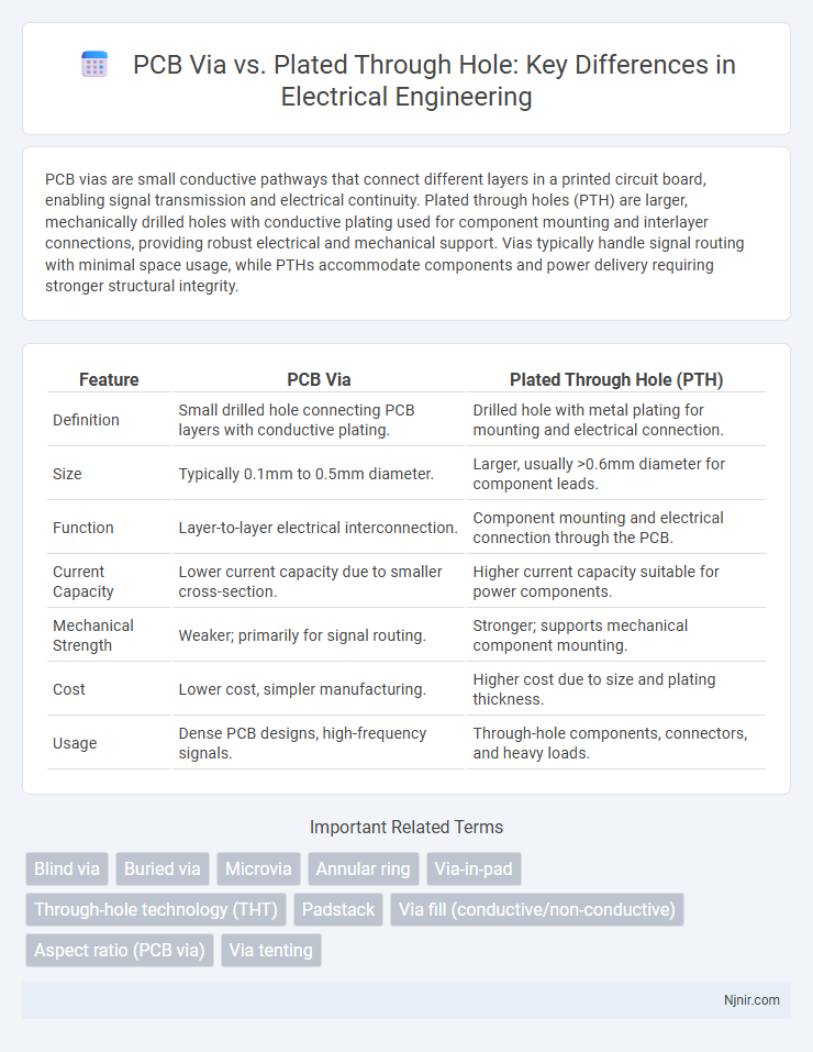
PCB vias are small conductive pathways that connect different layers in a printed circuit board, enabling signal transmission and electrical continuity. Plated through holes (PTH) are larger, mechanically drilled holes with conductive plating used for component mounting and interlayer connections, providing robust electrical and mechanical support. Vias typically handle signal routing with minimal space usage, while PTHs accommodate components and power delivery requiring stronger structural integrity.
Table of Comparison
| Feature | PCB Via | Plated Through Hole (PTH) |
|---|---|---|
| Definition | Small drilled hole connecting PCB layers with conductive plating. | Drilled hole with metal plating for mounting and electrical connection. |
| Size | Typically 0.1mm to 0.5mm diameter. | Larger, usually >0.6mm diameter for component leads. |
| Function | Layer-to-layer electrical interconnection. | Component mounting and electrical connection through the PCB. |
| Current Capacity | Lower current capacity due to smaller cross-section. | Higher current capacity suitable for power components. |
| Mechanical Strength | Weaker; primarily for signal routing. | Stronger; supports mechanical component mounting. |
| Cost | Lower cost, simpler manufacturing. | Higher cost due to size and plating thickness. |
| Usage | Dense PCB designs, high-frequency signals. | Through-hole components, connectors, and heavy loads. |
Introduction to PCB Vias and Plated Through Holes
PCB vias are small conductive pathways that connect different layers of a printed circuit board, enabling signal transfer and electrical connectivity. Plated through holes (PTHs) serve a similar function but are specifically drilled holes coated with a metal layer to ensure robust electrical conduction through the board thickness. Both PCB vias and PTHs are critical in multi-layer PCB design, affecting signal integrity, mechanical strength, and manufacturing complexity.
Structural Differences: Vias vs Plated Through Holes
Vias in PCBs are small, copper-plated holes that connect different layers of a multi-layer board, facilitating electrical continuity without component mounting. Plated Through Holes (PTH), in contrast, are larger holes that serve as mounting points for through-hole components while also providing electrical connectivity through copper plating. The key structural difference lies in size and purpose: vias primarily enable inter-layer signal routing, whereas PTHs combine mechanical support with electrical interconnection.
Electrical Conductivity Comparison
PCB vias and plated through holes (PTH) both serve as electrical connections between different layers of a printed circuit board, but their electrical conductivity varies due to construction differences. Vias typically have a smaller diameter and thinner copper plating, resulting in higher resistance compared to PTHs, which are larger and often feature thicker copper layers for enhanced conductivity and current-carrying capacity. When high electrical performance and minimal signal loss are critical, PTHs are preferred for their lower resistance and improved thermal dissipation over standard vias.
Manufacturing Processes and Costs
PCB vias are small, drilled holes filled or coated with conductive material to establish electrical connections between different layers, offering cost-effective manufacturing due to minimal material usage and simpler processes. Plated through holes (PTH), larger and mechanically robust, undergo a thorough electroplating process inside drilled holes, increasing production complexity and expense but enhancing reliability in high-current or mechanical stress applications. While PCB vias streamline manufacturing with automated drilling and plating techniques, PTH requires additional plating time and quality control, resulting in higher costs but improved durability for demanding electronic assemblies.
Mechanical Strength and Reliability
PCB vias offer mechanical strength through copper plating that reinforces the hole walls, ensuring reliable electrical connections across multiple layers. Plated through holes (PTHs) provide enhanced mechanical robustness by creating a continuous conductive path and strengthening hole integrity, which reduces the risk of cracks and delamination under stress. The reliability of PTHs surpasses that of simple vias in high-vibration or thermal cycling environments due to their thicker plating and structural support.
Applications: When to Use Vias or PTHs
Vias are ideal for high-density PCB designs requiring multiple signal layers and fine pitch connections, commonly used in multilayer boards to route signals between layers without occupying much space. Plated Through Holes (PTHs) serve well for mounting through-hole components and providing mechanical stability, often used in single or double-sided PCBs where component leads need secure soldering and reliable electrical connections. Choosing between vias and PTHs depends on design requirements such as signal integrity, mechanical strength, component type, and manufacturing cost constraints.
Impact on Signal Integrity
PCB vias and plated through holes (PTHs) both serve as electrical connections between layers but differ in their impact on signal integrity. Vias introduce parasitic inductance and capacitance, which can cause signal reflections and crosstalk, particularly at high frequencies, whereas PTHs, being larger and more robust, tend to have lower impedance discontinuities. Minimizing via stubs and optimizing via geometry are critical to preserving signal integrity in high-speed PCB designs.
Thermal Management Considerations
PCB vias and plated through holes (PTH) differ significantly in thermal management applications; vias, especially thermal vias, facilitate heat dissipation by connecting internal layers to heat sinks or ground planes, improving overall thermal conductivity. Plated through holes, with their robust copper plating along the hole walls, provide structural support and thermal paths but may introduce thermal resistance depending on plating thickness and hole diameter. Optimizing thermal management involves balancing via density, size, plating thickness, and placement relative to heat-generating components to ensure effective heat transfer and prevent thermal stress.
Design Guidelines for Optimal Usage
PCB vias must be carefully selected based on current carrying capacity and signal integrity requirements, with microvias preferred for high-density interconnects due to their smaller size and reduced parasitic inductance. Plated through holes (PTH) provide robust mechanical connections for component leads and power distribution, requiring adherence to drilling tolerances and plating thickness to prevent reliability issues like barrel voids or cracks. Design guidelines emphasize controlled annular ring dimensions, aspect ratios below 10:1, and proper via stubbing to optimize electrical performance and manufacturability.
Future Trends in PCB Interconnect Technology
PCB vias and plated through holes (PTH) remain integral to interconnect technology, with future trends emphasizing miniaturization and enhanced electrical performance. Advanced technologies like microvias and laser-drilled vias are driving higher density and finer pitch designs, crucial for next-generation high-speed and high-frequency applications. Emerging materials and surface treatments aim to improve reliability and signal integrity, enabling PCBs to meet evolving demands in aerospace, automotive, and IoT industries.
Blind via
Blind vias connect an outer PCB layer to one or more inner layers without passing through the entire board, offering better signal integrity and space-saving advantages compared to plated through holes that traverse the full board thickness.
Buried via
Buried vias in PCBs provide high-density interlayer connections hidden within internal layers, unlike plated through holes that extend through the entire board, optimizing space and signal integrity in complex multilayer designs.
Microvia
Microvias are small-diameter plated through holes used in PCBs to achieve high-density interconnections with minimal electrical resistance and improved signal integrity compared to traditional plated through holes.
Annular ring
The annular ring, the copper area surrounding a PCB via or plated through hole, is critical for ensuring reliable electrical connectivity and mechanical strength, with plated through holes typically requiring larger annular rings for enhanced durability and signal integrity.
Via-in-pad
Via-in-pad offers superior signal integrity and minimized parasitic inductance compared to traditional plated through holes by embedding vias directly within component pads, optimizing high-density PCB designs.
Through-hole technology (THT)
Through-hole technology (THT) utilizes plated through holes (PTH) to electrically connect multiple PCB layers, whereas vias mainly serve as conductive pathways without component mounting.
Padstack
PCB via padstack is specifically designed for electrical connectivity between layers with smaller annular rings and optimized drill sizes, while plated through hole padstack prioritizes mechanical stability and component mounting with larger pads and consistent plating thickness.
Via fill (conductive/non-conductive)
PCB vias typically feature conductive or non-conductive via fill materials to enhance electrical performance, mechanical strength, and thermal management, whereas plated through holes are primarily metallized to establish robust electrical connections through the board layers without fill.
Aspect ratio (PCB via)
PCB vias typically feature a lower aspect ratio than plated through holes, enhancing signal integrity and manufacturability by reducing drill depth relative to hole diameter.
Via tenting
Via tenting in PCB design involves covering plated through holes with solder mask to prevent solder wicking, enhance protection against contaminants, and improve reliability compared to standard vias and plated through holes.
PCB via vs plated through hole Infographic