PNP and NPN transistors differ primarily in their charge carrier types and current flow directions, with PNP transistors using holes as the majority carriers and NPN transistors using electrons. NPN transistors are generally preferred for high-speed switching due to higher electron mobility, while PNP transistors are commonly used in low-side switching applications. Understanding their distinct polarity requirements and biasing conditions is essential for designing reliable and efficient electronic circuits.
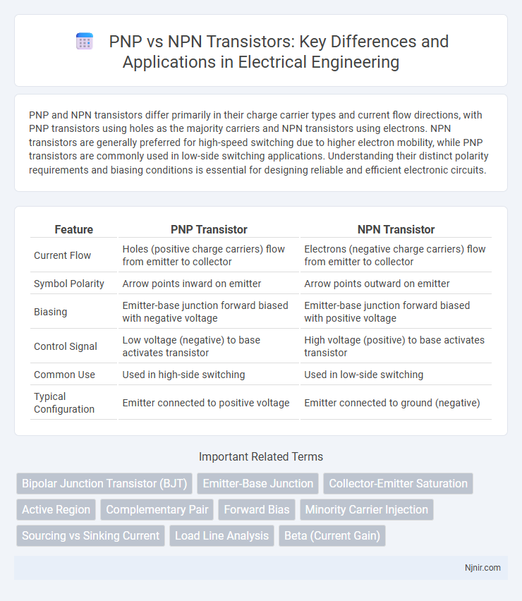
Table of Comparison
| Feature | PNP Transistor | NPN Transistor |
|---|---|---|
| Current Flow | Holes (positive charge carriers) flow from emitter to collector | Electrons (negative charge carriers) flow from emitter to collector |
| Symbol Polarity | Arrow points inward on emitter | Arrow points outward on emitter |
| Biasing | Emitter-base junction forward biased with negative voltage | Emitter-base junction forward biased with positive voltage |
| Control Signal | Low voltage (negative) to base activates transistor | High voltage (positive) to base activates transistor |
| Common Use | Used in high-side switching | Used in low-side switching |
| Typical Configuration | Emitter connected to positive voltage | Emitter connected to ground (negative) |
Introduction to PNP and NPN Transistors
PNP and NPN transistors are bipolar junction transistors (BJTs) that control current flow through different polarities of voltage. NPN transistors consist of a layer of p-type semiconductor sandwiched between two n-type layers, allowing current to flow when the base is positively biased relative to the emitter. In contrast, PNP transistors have a layer of n-type semiconductor between two p-type layers and conduct current when the base is negatively biased compared to the emitter.
Fundamental Working Principles
PNP and NPN transistors operate based on the movement of charge carriers within their semiconductor layers; NPN transistors use electrons as majority carriers flowing from the emitter to the collector, while PNP transistors rely on holes moving from the emitter to the collector. The fundamental working principle involves the base-emitter junction being forward biased and the base-collector junction being reverse biased, enabling control of a large current between emitter and collector through a small base current. Electron flow in NPN transistors corresponds to conventional current flow in PNP transistors, resulting in opposite polarities for power supply connections and signal inputs in circuit designs.
Symbol and Pin Configuration
PNP and NPN transistors are bipolar junction transistors (BJTs) distinguished by their symbol orientations and pin configurations. The PNP transistor symbol features an arrow on the emitter pointing inward toward the base, while the NPN transistor symbol shows the arrow pointing outward from the emitter; this arrow direction indicates the conventional current flow. In standard transistor packages, pin configuration typically places the emitter, base, and collector in a specific order, but this arrangement can vary by manufacturer and model, making datasheet verification essential for correct circuit integration.
Key Differences Between PNP and NPN
PNP and NPN transistors differ primarily in their charge carrier types and current flow directions, with PNP using holes as majority carriers and NPN using electrons. In NPN transistors, current flows from the collector to the emitter, while in PNP transistors, it flows from the emitter to the collector. NPN transistors are generally preferred for switching and amplification due to higher electron mobility, whereas PNP transistors are used in complementary configurations.
Electrical Characteristics Comparison
PNP and NPN transistors differ primarily in their electrical characteristics, with NPN transistors typically having electrons as the majority charge carriers, resulting in higher electron mobility and faster switching speeds compared to PNP transistors, which rely on holes as majority carriers. The voltage polarity for PNP transistors is opposite to that of NPN transistors; PNP transistors require a negative base-emitter voltage to turn on, whereas NPN transistors require a positive base-emitter voltage. Current flow in NPN transistors occurs from collector to emitter, while in PNP transistors, it flows from emitter to collector, affecting the design and polarity requirements in circuits.
Applications of PNP Transistors
PNP transistors are widely used in high-side switch applications where the load is connected to the ground, allowing current to flow from the emitter to the collector when the base is pulled low. They are commonly found in relay drivers, amplifier circuits, and in circuits requiring positive voltage control and reverse polarity protection. Their ability to source current makes them ideal for controlling devices in automotive electronics and power management systems.
Applications of NPN Transistors
NPN transistors are widely used in switching applications due to their ability to efficiently control current flow from the collector to the emitter when a positive voltage is applied to the base. They are commonly found in digital circuits, amplification systems, and power regulation devices where fast switching speeds and high gain are essential. Industrial automation and consumer electronics frequently utilize NPN transistors for driving loads such as relays, LEDs, and motors.
Selection Criteria: PNP vs NPN
Selection criteria for PNP versus NPN transistors depend on the required current flow and circuit configuration, as NPN transistors are preferred for low-side switching with electrons as majority carriers, providing higher mobility and faster operation. PNP transistors suit high-side switching applications where positive voltage control is needed, with holes as majority carriers enabling simpler sourcing of current in certain circuits. Consideration of voltage polarity, gain, frequency response, and load placement is essential when choosing between PNP and NPN transistors for optimal device performance and reliability.
Circuit Design Considerations
PNP and NPN transistors differ primarily in polarity and current flow, affecting circuit design considerations such as biasing and load placement. NPN transistors typically source current from the collector to emitter and require a positive base voltage relative to the emitter, making them ideal for low-side switching, while PNP transistors sink current and need a negative base voltage relative to the emitter, suitable for high-side switching. Selecting between PNP and NPN also influences the type of power supply and control signals used, impacting overall circuit complexity and efficiency.
Conclusion: Choosing Between PNP and NPN Transistors
NPN transistors are typically preferred in circuits requiring fast switching and better electron mobility, while PNP transistors are advantageous in low-side switching and positive ground applications. The choice between the two depends on the specific circuit configuration, voltage requirements, and polarity of the power supply. Understanding the electrical characteristics and intended use case ensures optimal transistor selection for reliable and efficient performance.
Bipolar Junction Transistor (BJT)
PNP and NPN Bipolar Junction Transistors (BJTs) differ primarily in their charge carrier flow, with NPN transistors using electrons as majority carriers for faster switching and higher efficiency, while PNP transistors use holes and are typically employed in complementary or high-side switching circuits.
Emitter-Base Junction
The emitter-base junction of a PNP transistor consists of a forward-biased P-type emitter and N-type base, while in an NPN transistor, it is a forward-biased N-type emitter and P-type base.
Collector-Emitter Saturation
PNP transistors exhibit a positive voltage drop across the collector-emitter saturation region typically around 0.2V to 0.4V, whereas NPN transistors generally have a slightly lower collector-emitter saturation voltage, enhancing efficiency in switching applications.
Active Region
In the active region, an NPN transistor allows current flow from the collector to the emitter when the base is positively biased relative to the emitter, whereas a PNP transistor conducts current from the emitter to the collector when the base is negatively biased relative to the emitter.
Complementary Pair
PNP and NPN transistors form a complementary pair essential for push-pull amplifier circuits, enabling efficient current flow control with opposite polarity voltage and current directions.
Forward Bias
Forward bias in PNP transistors occurs when the emitter is at a higher potential than the base, allowing hole flow from emitter to base, whereas in NPN transistors, forward bias requires the base to be at a higher potential than the emitter, enabling electron flow from emitter to base.
Minority Carrier Injection
PNP transistors inject minority carriers (holes) from the emitter into the base, while NPN transistors inject minority carriers (electrons) from the emitter into the base, significantly influencing their current flow and switching characteristics.
Sourcing vs Sinking Current
PNP transistors source current by supplying it from the emitter to the load, while NPN transistors sink current by drawing it from the load into the collector.
Load Line Analysis
Load line analysis of PNP and NPN transistors reveals the operating point by graphing the device's characteristic curves with the external circuit constraints, showing how current and voltage vary across the transistor in different configurations.
Beta (Current Gain)
PNP and NPN transistors both exhibit current gain (Beta), with NPN transistors typically offering slightly higher Beta values due to better electron mobility compared to the hole mobility in PNP transistors.
PNP vs NPN (transistor) Infographic