A ground plane and a power plane serve distinct roles in PCB design, with the ground plane providing a common reference point and minimizing electromagnetic interference, while the power plane distributes voltage uniformly across the circuit. Effective separation of these planes reduces noise coupling and improves signal integrity, essential for high-frequency applications. Optimizing their placement and layer stacking enhances overall electrical performance and thermal management.
Table of Comparison
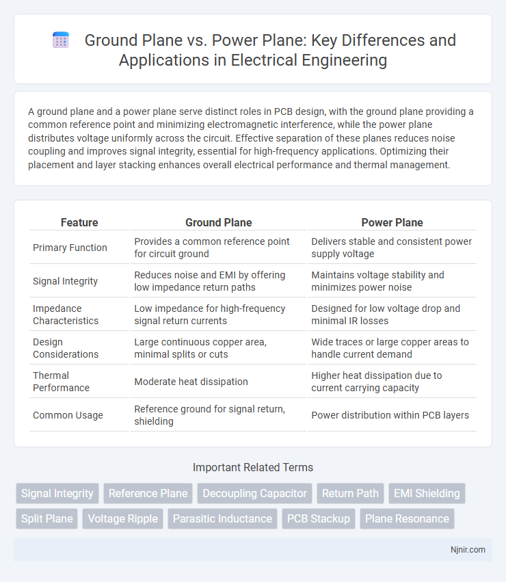
| Feature | Ground Plane | Power Plane |
|---|---|---|
| Primary Function | Provides a common reference point for circuit ground | Delivers stable and consistent power supply voltage |
| Signal Integrity | Reduces noise and EMI by offering low impedance return paths | Maintains voltage stability and minimizes power noise |
| Impedance Characteristics | Low impedance for high-frequency signal return currents | Designed for low voltage drop and minimal IR losses |
| Design Considerations | Large continuous copper area, minimal splits or cuts | Wide traces or large copper areas to handle current demand |
| Thermal Performance | Moderate heat dissipation | Higher heat dissipation due to current carrying capacity |
| Common Usage | Reference ground for signal return, shielding | Power distribution within PCB layers |
Introduction to Ground Plane and Power Plane
Ground planes and power planes are essential components in PCB design, serving as reference layers for voltage and signal integrity. A ground plane provides a stable 0V reference, minimizing noise and EMI by offering a low-impedance return path for current. Power planes carry the supply voltage across the board, ensuring consistent power delivery and reducing voltage drops in complex electronic circuits.
Fundamental Roles in PCB Design
Ground planes provide a low-impedance return path for signals, reducing electromagnetic interference (EMI) and improving signal integrity in PCB designs. Power planes distribute stable voltage levels with minimal noise and voltage drops, ensuring efficient power delivery to all components. Both planes are essential for maintaining electrical performance, minimizing crosstalk, and enhancing overall circuit reliability.
Key Differences Between Ground and Power Planes
Ground planes provide a reference voltage level, typically zero volts, ensuring signal integrity and minimizing electrical noise in printed circuit boards (PCBs). Power planes distribute the supply voltage uniformly across different components, maintaining consistent power delivery and reducing voltage drops. Key differences include their electrical roles, with ground planes acting as return paths for current, while power planes supply active voltage levels, requiring distinct design considerations to optimize performance and minimize interference.
Material Selection for Ground vs Power Planes
Ground planes typically utilize copper or aluminum with high conductivity and low resistivity to ensure minimal voltage drops and effective grounding, while power planes require materials that handle higher current densities and thermal management, often incorporating thicker copper layers or copper-clad laminates. Dielectric materials for ground and power planes are chosen based on their dielectric constant and thermal stability to minimize signal interference and maintain integrity under electrical stress. Selecting appropriate PCB substrate materials like FR-4 or high-frequency laminates directly influences the performance and reliability of both ground and power planes in electronic circuits.
Impact on Signal Integrity
Ground planes provide a reference voltage that minimizes electromagnetic interference (EMI) and reduces signal noise, ensuring stable signal integrity in high-speed circuits. Power planes deliver consistent voltage levels but can introduce power supply noise that affects signal quality if not properly decoupled. Proper separation and careful layout of ground and power planes are critical to minimizing crosstalk, maintaining signal return paths, and enhancing overall signal integrity in PCB design.
Effects on Electromagnetic Interference (EMI)
Ground planes significantly reduce electromagnetic interference (EMI) by providing a low-impedance return path for signals, minimizing loop area and radiated emissions. Power planes, while essential for stable voltage distribution, can contribute to EMI if not properly decoupled and segmented, as noise may couple into sensitive signal layers. Effective PCB design often employs separate ground and power planes with careful placement of decoupling capacitors to mitigate EMI and maintain signal integrity.
Thermal Management Considerations
Ground planes provide efficient heat dissipation due to their extensive copper coverage, improving thermal conductivity and lowering component temperatures on PCBs. Power planes also contribute to heat spreading but typically involve higher current densities, which may generate localized hotspots requiring careful thermal relief design. Proper balance between ground and power plane copper thickness and thermal vias enhances overall thermal management in multilayer circuit boards.
Layer Stack-Up Strategies
Ground planes serve as reference layers providing a low-inductance return path crucial for signal integrity, while power planes distribute voltage with minimal noise across the PCB. Effective layer stack-up strategies place ground planes adjacent to signal layers to reduce electromagnetic interference (EMI), and position power planes between ground planes to enhance power distribution and minimize voltage fluctuations. Optimizing the arrangement of ground and power planes in multilayer PCBs significantly improves signal integrity, reduces crosstalk, and enhances overall electromagnetic compatibility (EMC).
Design Best Practices
Ground plane and power plane design best practices emphasize minimizing noise and ensuring stable voltage distribution. A continuous, unbroken ground plane reduces electromagnetic interference (EMI) and provides a low-inductance return path for signals, while a solid power plane with proper decoupling capacitors maintains consistent voltage levels. Maintaining proper spacing between ground and power planes, using multiple layers, and careful layout integration enhances signal integrity and overall PCB performance.
Common Mistakes and How to Avoid Them
Common mistakes in distinguishing ground planes from power planes include improper separation, which can cause noise coupling and impedance issues, and insufficient grounding that leads to signal integrity problems. Avoid these pitfalls by clearly defining and isolating ground and power planes in PCB layout, ensuring continuous and low-impedance ground paths, and using proper decoupling techniques to maintain stable voltage levels. Implementing careful layer stack-up planning and adhering to high-frequency design principles improves overall electromagnetic compatibility and reduces interference.
Signal Integrity
A continuous ground plane enhances signal integrity by minimizing impedance discontinuities and reducing electromagnetic interference compared to segmented power planes.
Reference Plane
A ground plane provides a stable 0V reference for signal integrity while a power plane delivers regulated voltage, with both serving as crucial reference planes in PCB design to minimize noise and ensure reliable circuit operation.
Decoupling Capacitor
Decoupling capacitors placed between ground planes and power planes minimize noise and stabilize voltage by providing low-impedance paths for high-frequency currents.
Return Path
The ground plane offers a low-impedance return path for signals, minimizing noise and electromagnetic interference compared to the power plane, which primarily distributes voltage and may not provide an optimal return path.
EMI Shielding
A dedicated ground plane provides superior EMI shielding by minimizing impedance and creating a low-inductance return path compared to a power plane, which primarily distributes voltage and may introduce noise coupling.
Split Plane
A split plane in PCB design refers to a ground or power plane divided into separate regions to accommodate different voltage domains or signal return paths, potentially causing increased EMI and impedance discontinuities if not properly managed.
Voltage Ripple
A ground plane minimizes voltage ripple by providing a low-impedance return path and reducing electromagnetic interference, whereas a power plane directly distributes voltage but may introduce higher ripple due to less effective noise suppression.
Parasitic Inductance
Ground planes exhibit lower parasitic inductance than power planes, enhancing signal integrity and reducing electromagnetic interference in high-frequency PCB designs.
PCB Stackup
A well-designed PCB stackup balances Ground Plane and Power Plane layers to minimize noise, improve signal integrity, and optimize electromagnetic compatibility.
Plane Resonance
Plane resonance occurs when the Ground Plane and Power Plane form a parallel-plate capacitor with an inductive loop, causing impedance peaks that degrade high-frequency performance in PCB designs.
Ground Plane vs Power Plane Infographic