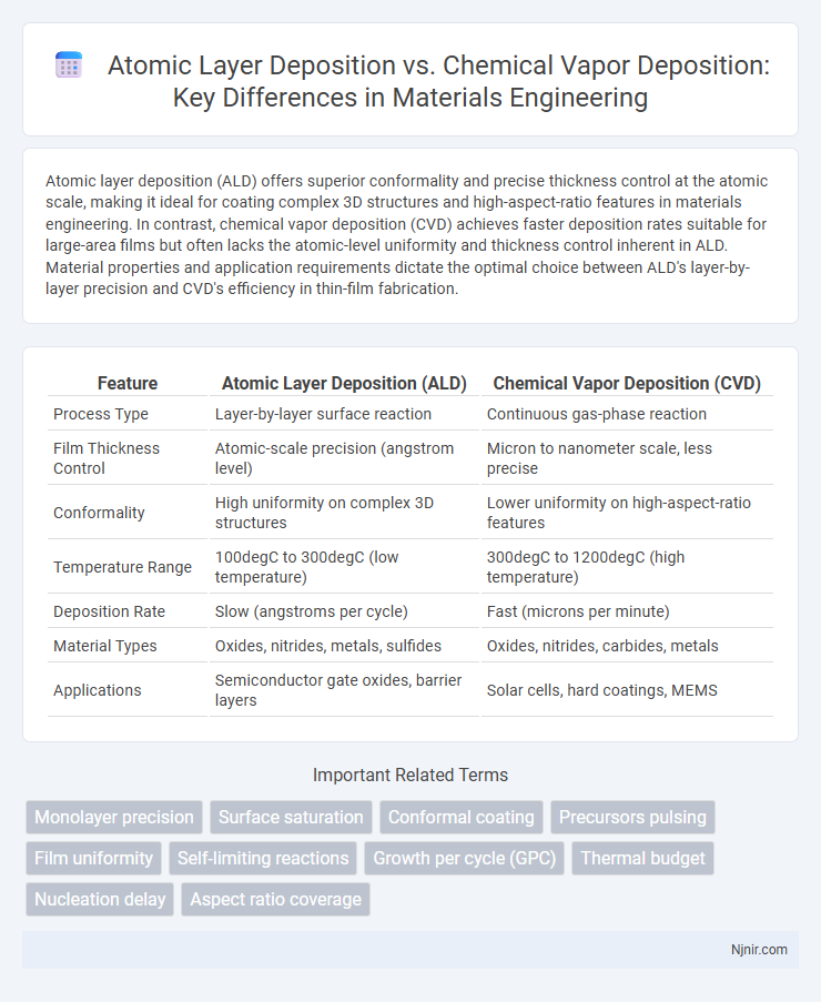
Atomic layer deposition (ALD) offers superior conformality and precise thickness control at the atomic scale, making it ideal for coating complex 3D structures and high-aspect-ratio features in materials engineering. In contrast, chemical vapor deposition (CVD) achieves faster deposition rates suitable for large-area films but often lacks the atomic-level uniformity and thickness control inherent in ALD. Material properties and application requirements dictate the optimal choice between ALD's layer-by-layer precision and CVD's efficiency in thin-film fabrication.
Table of Comparison
| Feature | Atomic Layer Deposition (ALD) | Chemical Vapor Deposition (CVD) |
|---|---|---|
| Process Type | Layer-by-layer surface reaction | Continuous gas-phase reaction |
| Film Thickness Control | Atomic-scale precision (angstrom level) | Micron to nanometer scale, less precise |
| Conformality | High uniformity on complex 3D structures | Lower uniformity on high-aspect-ratio features |
| Temperature Range | 100degC to 300degC (low temperature) | 300degC to 1200degC (high temperature) |
| Deposition Rate | Slow (angstroms per cycle) | Fast (microns per minute) |
| Material Types | Oxides, nitrides, metals, sulfides | Oxides, nitrides, carbides, metals |
| Applications | Semiconductor gate oxides, barrier layers | Solar cells, hard coatings, MEMS |
Introduction to Atomic Layer Deposition and Chemical Vapor Deposition
Atomic Layer Deposition (ALD) is a thin-film deposition technique characterized by its self-limiting surface reactions, enabling atomic-scale thickness control and uniformity on complex 3D structures. Chemical Vapor Deposition (CVD) involves chemical reactions of gaseous precursors on a substrate, producing high-quality films with faster deposition rates but less precise thickness control. ALD offers unparalleled conformality and film uniformity compared to CVD, which remains advantageous for large-scale, high-throughput applications.
Fundamental Principles of ALD and CVD
Atomic Layer Deposition (ALD) is based on sequential, self-limiting surface reactions that deposit atomic layers one at a time, ensuring precise thickness control and uniformity. Chemical Vapor Deposition (CVD) involves continuous chemical reactions of gaseous precursors on a heated substrate, producing a thin film through nucleation and growth processes. While ALD relies on surface saturation and pulse exposure to control film growth, CVD depends on precursor diffusion, reaction kinetics, and thermal energy to achieve film deposition.
Process Mechanisms: Sequential vs. Continuous Reactions
Atomic Layer Deposition (ALD) operates through sequential, self-limiting surface reactions that deposit material one atomic layer at a time, ensuring precise thickness control and uniformity. Chemical Vapor Deposition (CVD) involves continuous gas-phase reactions and surface adsorption that result in film growth, allowing faster deposition but with less atomic-level precision. The distinct process mechanisms affect film conformity, with ALD excelling in coating complex 3D structures due to its layer-by-layer approach versus CVD's reliance on continuous precursor flow.
Material Compatibility and Substrate Versatility
Atomic layer deposition (ALD) offers superior material compatibility by enabling precise, conformal coatings on complex 3D structures and temperature-sensitive substrates, making it ideal for semiconductor and nanotechnology applications. Chemical vapor deposition (CVD) supports a broader range of materials and can deposit thicker films at higher rates but may struggle with uniformity on non-planar surfaces and delicate substrates. ALD's self-limiting surface reactions enhance substrate versatility, enabling high-quality thin films on metals, oxides, and polymers, whereas CVD requires careful control of process parameters to avoid substrate damage and ensure adhesion.
Film Thickness Control and Uniformity
Atomic Layer Deposition (ALD) offers unparalleled film thickness control at the atomic scale through self-limiting surface reactions, enabling consistent layer-by-layer growth and uniformity across complex 3D structures. Chemical Vapor Deposition (CVD) achieves higher deposition rates but often results in less precise thickness control and potential non-uniformity due to gas-phase reactions and shadowing effects on intricate topographies. ALD's superior uniformity and conformality make it ideal for applications demanding nanoscale precision and consistent thin films over large areas.
Applications in Advanced Materials Engineering
Atomic layer deposition (ALD) offers atomic-scale thickness control and conformal coatings, making it ideal for semiconductor fabrication, high-k dielectric layers, and complex 3D nanostructures. Chemical vapor deposition (CVD) enables high-throughput production of uniform thin films over large areas, widely used in photovoltaic cells, graphene synthesis, and protective coatings for advanced aerospace materials. Both techniques are crucial for developing next-generation electronic devices, energy storage systems, and wearable sensors due to their precise film quality and versatility in material composition.
Equipment and Process Complexity
Atomic layer deposition (ALD) equipment features precise, sequential gas flow and self-limiting surface reactions, requiring complex control systems for ultrathin film uniformity at the atomic scale. Chemical vapor deposition (CVD) systems operate with continuous gas flow and higher deposition rates but involve less intricate control over monolayer thickness, resulting in comparatively simpler equipment design. ALD's process complexity supports superior conformality on 3D structures, whereas CVD trades off complexity for throughput and scalability in various material depositions.
Advantages and Limitations of ALD vs. CVD
Atomic Layer Deposition (ALD) offers unparalleled thickness control and conformality on complex 3D nanostructures, providing atomic-scale precision critical for advanced semiconductor and coating applications. Chemical Vapor Deposition (CVD) enables faster deposition rates and is more suitable for high-throughput manufacturing of relatively planar surfaces but lacks the uniformity and step coverage of ALD on high-aspect-ratio features. Limitations of ALD include slower deposition speeds and higher costs, while CVD faces challenges with film uniformity, especially on uneven or nanoscale substrates.
Environmental Impact and Cost Considerations
Atomic layer deposition (ALD) offers superior material efficiency and reduced waste generation compared to chemical vapor deposition (CVD), making it more environmentally friendly, especially for thin films and nanoscale applications. While ALD equipment and precursor costs are higher, its precise control over film thickness minimizes material usage and rework expenses. In contrast, CVD typically involves higher precursor consumption and energy use but benefits from faster deposition rates, resulting in lower operational costs for large-scale production.
Future Trends in Thin Film Deposition Technologies
Future trends in thin film deposition technologies emphasize atomic layer deposition (ALD) for its unparalleled precision in layer thickness and conformality at the atomic scale, making it ideal for advanced semiconductor manufacturing and nanotechnology applications. Chemical vapor deposition (CVD) continues to evolve with innovations in plasma-enhanced CVD and low-temperature processes, enhancing film quality and reducing thermal budgets for flexible electronics and 3D device architectures. Emerging hybrid techniques combining ALD and CVD principles aim to optimize throughput and material properties, driving next-generation thin films in energy storage, microelectronics, and optoelectronics.
Monolayer precision
Atomic layer deposition enables monolayer precision through sequential self-limiting surface reactions, whereas chemical vapor deposition typically results in less controlled, multilayer film growth.
Surface saturation
Atomic layer deposition achieves precise surface saturation through self-limiting reactions, ensuring uniform thin films, while chemical vapor deposition relies on continuous precursor flow leading to less controlled surface coverage.
Conformal coating
Atomic layer deposition provides superior conformal coating with precise thickness control on complex 3D structures compared to chemical vapor deposition.
Precursors pulsing
Atomic layer deposition precisely controls film thickness through sequential precursor pulsing and surface reactions, while chemical vapor deposition uses continuous precursor flow resulting in less atomic-level thickness control.
Film uniformity
Atomic layer deposition achieves superior film uniformity with atomic-scale thickness control compared to chemical vapor deposition, which often results in less uniform films due to precursor depletion and surface reaction variability.
Self-limiting reactions
Atomic layer deposition utilizes self-limiting surface reactions to achieve precise atomic-scale film thickness control, whereas chemical vapor deposition relies on continuous chemical reactions without inherent self-limiting mechanisms.
Growth per cycle (GPC)
Atomic layer deposition (ALD) provides precise, self-limiting growth per cycle (GPC) typically in the range of 0.1 to 0.3 nm, enabling atomic-scale thickness control, whereas chemical vapor deposition (CVD) offers higher GPC but with less uniformity and conformality at the nanoscale.
Thermal budget
Atomic layer deposition (ALD) offers a significantly lower thermal budget by enabling precise, layer-by-layer film growth at temperatures typically between 100-300degC, compared to chemical vapor deposition (CVD), which often requires higher temperatures ranging from 300-1000degC, impacting substrate compatibility and thermal-induced stress.
Nucleation delay
Atomic layer deposition exhibits minimal nucleation delay due to its self-limiting surface reactions, while chemical vapor deposition often experiences longer nucleation delays caused by continuous precursor decomposition and surface saturation dynamics.
Aspect ratio coverage
Atomic layer deposition (ALD) achieves superior aspect ratio coverage compared to chemical vapor deposition (CVD) due to its self-limiting surface reactions enabling uniform, conformal thin films in high-aspect-ratio nanostructures.
atomic layer deposition vs chemical vapor deposition Infographic