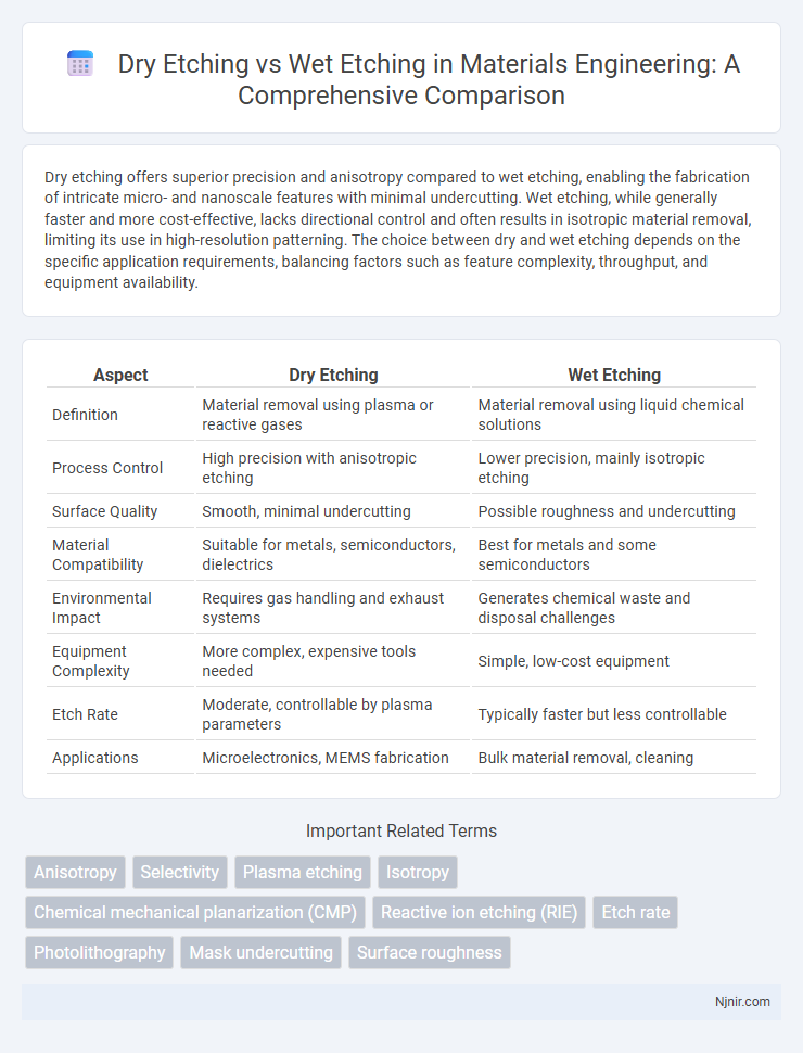
Dry etching offers superior precision and anisotropy compared to wet etching, enabling the fabrication of intricate micro- and nanoscale features with minimal undercutting. Wet etching, while generally faster and more cost-effective, lacks directional control and often results in isotropic material removal, limiting its use in high-resolution patterning. The choice between dry and wet etching depends on the specific application requirements, balancing factors such as feature complexity, throughput, and equipment availability.
Table of Comparison
| Aspect | Dry Etching | Wet Etching |
|---|---|---|
| Definition | Material removal using plasma or reactive gases | Material removal using liquid chemical solutions |
| Process Control | High precision with anisotropic etching | Lower precision, mainly isotropic etching |
| Surface Quality | Smooth, minimal undercutting | Possible roughness and undercutting |
| Material Compatibility | Suitable for metals, semiconductors, dielectrics | Best for metals and some semiconductors |
| Environmental Impact | Requires gas handling and exhaust systems | Generates chemical waste and disposal challenges |
| Equipment Complexity | More complex, expensive tools needed | Simple, low-cost equipment |
| Etch Rate | Moderate, controllable by plasma parameters | Typically faster but less controllable |
| Applications | Microelectronics, MEMS fabrication | Bulk material removal, cleaning |
Introduction to Etching Techniques in Materials Engineering
Dry etching utilizes plasma or reactive gases to remove material from a substrate with high precision, making it ideal for microfabrication in semiconductor industries. Wet etching, involving liquid chemical solutions, offers simple and cost-effective material removal but with less control over etch profiles and potential undercutting. Both techniques play crucial roles in materials engineering by enabling selective material patterning and surface modification based on application-specific requirements.
Fundamentals of Dry Etching
Dry etching is a plasma-based process that uses reactive ions to precisely remove material from the substrate, offering superior anisotropy compared to wet etching. It allows for fine pattern transfer and enhanced control over etch depth and profile, critical for semiconductor fabrication and nanotechnology applications. Key parameters such as gas composition, pressure, RF power, and substrate temperature are finely tuned to optimize etch rate, selectivity, and surface damage.
Fundamentals of Wet Etching
Wet etching involves the use of liquid chemical solutions to selectively remove material from a substrate by dissolving specific layers, relying on chemical reactions at the surface. It is characterized by isotropic etching profiles, where the etch rate is generally uniform in all directions, making it suitable for applications requiring smooth, large-area material removal. Key parameters influencing wet etching include solution concentration, temperature, agitation, and etchant selectivity relative to the substrate and mask materials.
Chemical Reactions and Mechanisms
Dry etching employs plasma or reactive gases to chemically react with a material's surface, forming volatile by-products that are then removed, enabling precise anisotropic etching. Wet etching involves liquid chemical solutions that dissolve material isotropically through surface reactions and etch rate depends heavily on concentration, temperature, and material compatibility. The mechanisms in dry etching combine physical bombardment and chemical reactions, whereas wet etching relies solely on chemical dissolution processes.
Process Parameters and Control
Dry etching utilizes plasma or reactive gases to precisely control etch rates, anisotropy, and selectivity through parameters like gas composition, pressure, RF power, and temperature, offering superior spatial resolution and uniformity. Wet etching depends on chemical solutions, where factors such as concentration, temperature, and agitation dictate etch rate and isotropy but often lack the fine control achievable in dry etching. Process control in dry etching benefits from real-time monitoring and precise parameter adjustment, whereas wet etching relies more on fixed bath conditions and time, making dry etching preferable for advanced semiconductor fabrication requiring high precision.
Material Compatibility and Selectivity
Dry etching offers higher material compatibility and selectivity compared to wet etching due to its use of plasma or reactive gases that precisely target specific materials without affecting adjacent layers. Wet etching often relies on chemical solutions that can indiscriminately dissolve multiple materials, reducing process control and selectivity. Advanced dry etching techniques, such as reactive ion etching (RIE), enable superior pattern fidelity and enable etching of complex materials like silicon nitride and oxides with minimal undercutting.
Surface Morphology and Etch Profiles
Dry etching provides superior control over surface morphology with anisotropic etch profiles, enabling precise pattern transfer and minimal undercutting on substrate materials like silicon and GaAs. Wet etching typically results in isotropic etch profiles, causing more pronounced undercut and rougher surface textures due to chemical diffusion and reaction rates. Optimizing plasma parameters in dry etching enhances feature resolution critical for microfabrication, whereas wet etching remains suitable for applications tolerating less dimensional accuracy.
Applications in Semiconductor Manufacturing
Dry etching is widely used in semiconductor manufacturing for precise pattern transfer and high-resolution feature definition, especially in advanced CMOS and MEMS fabrication processes. Wet etching is favored for applications requiring isotropic material removal and simpler process setups, such as cleaning and bulk material removal in less complex device structures. Both techniques are crucial depending on the required etch profile, selectivity, and material compatibility in semiconductor device fabrication.
Advantages and Limitations of Dry vs Wet Etching
Dry etching offers precise anisotropic patterns with high resolution, making it ideal for microfabrication processes requiring fine features and clean sidewalls, while wet etching provides faster material removal and simpler setup but often results in isotropic etching with less control over feature dimensions. Dry etching enables compatibility with complex multilayer structures and produces less undercutting, enhancing device performance in semiconductor manufacturing, whereas wet etching's chemical selectivity can be limited and may cause surface roughness or damage sensitive materials. Limitations of dry etching include higher equipment cost and potential plasma-induced damage, while wet etching faces challenges with uniformity, reproducibility, and disposal of hazardous chemicals.
Future Trends in Etching Technologies
Future trends in etching technologies emphasize the integration of atomic layer etching (ALE) for enhanced precision and reduced damage in semiconductor fabrication. Advances in plasma-based dry etching processes focus on improving selectivity and anisotropy while minimizing environmental impact through eco-friendly gases. Wet etching methods are evolving with the development of novel chemical formulations that enable higher throughput and better compatibility with emerging materials like 2D semiconductors.
Anisotropy
Dry etching offers superior anisotropy compared to wet etching, enabling precise, vertical sidewall profiles essential for advanced semiconductor device fabrication.
Selectivity
Dry etching offers higher selectivity than wet etching by precisely controlling plasma chemistry and ion energy to target specific materials without damaging adjacent layers.
Plasma etching
Plasma etching, a dry etching method, offers precise anisotropic material removal and superior pattern fidelity compared to the isotropic nature of wet etching, making it essential for advanced semiconductor fabrication.
Isotropy
Wet etching is typically isotropic, resulting in uniform material removal in all directions, whereas dry etching offers anisotropic profiles with greater directional control for precise microfabrication.
Chemical mechanical planarization (CMP)
Chemical mechanical planarization (CMP) complements dry etching by providing superior surface planarity and uniformity, whereas wet etching often lacks the precision and control needed for advanced semiconductor fabrication.
Reactive ion etching (RIE)
Reactive ion etching (RIE) offers precise anisotropic etching with superior control over feature dimensions compared to wet etching methods, making it essential for high-resolution semiconductor fabrication.
Etch rate
Dry etching typically offers higher etch rates and greater anisotropy compared to wet etching, which generally exhibits slower etch rates and isotropic profiles.
Photolithography
Dry etching offers precise anisotropic pattern transfer with superior control over feature dimensions in photolithography compared to the isotropic nature of wet etching, making it essential for advanced semiconductor fabrication.
Mask undercutting
Dry etching minimizes mask undercutting by using directional plasma ions, whereas wet etching often causes significant mask undercutting due to isotropic chemical reactions.
Surface roughness
Dry etching typically results in lower surface roughness compared to wet etching, offering more precise and controlled material removal for advanced microfabrication processes.
dry etching vs wet etching Infographic