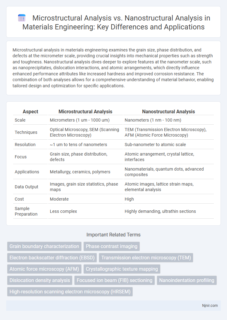
Microstructural analysis in materials engineering examines the grain size, phase distribution, and defects at the micrometer scale, providing crucial insights into mechanical properties such as strength and toughness. Nanostructural analysis dives deeper to explore features at the nanometer scale, such as nanoprecipitates, dislocation interactions, and atomic arrangements, which directly influence enhanced performance attributes like increased hardness and improved corrosion resistance. The combination of both analyses allows for a comprehensive understanding of material behavior, enabling tailored design and optimization for specific applications.
Table of Comparison
| Aspect | Microstructural Analysis | Nanostructural Analysis |
|---|---|---|
| Scale | Micrometers (1 um - 1000 um) | Nanometers (1 nm - 100 nm) |
| Techniques | Optical Microscopy, SEM (Scanning Electron Microscopy) | TEM (Transmission Electron Microscopy), AFM (Atomic Force Microscopy) |
| Resolution | ~1 um to tens of nanometers | Sub-nanometer to atomic scale |
| Focus | Grain size, phase distribution, defects | Atomic arrangement, crystal lattice, interfaces |
| Applications | Metallurgy, ceramics, polymers | Nanomaterials, quantum dots, advanced composites |
| Data Output | Images, grain size statistics, phase maps | Atomic images, lattice strain maps, elemental analysis |
| Cost | Moderate | High |
| Sample Preparation | Less complex | Highly demanding, ultrathin sections |
Introduction to Microstructural and Nanostructural Analysis
Microstructural analysis examines the physical and chemical structure of materials at the micrometer scale, revealing grain size, phase distribution, and defects critical for mechanical properties. Nanostructural analysis delves deeper into structures below 100 nanometers, enabling the study of atomic arrangements, nanoparticles, and interfaces influencing electronic and optical behaviors. Both techniques employ advanced microscopy methods like scanning electron microscopy (SEM) for microstructures and transmission electron microscopy (TEM) for nanostructures, essential for material science research and development.
Scale Differences: Microstructure vs Nanostructure
Microstructural analysis examines features ranging from approximately 1 micrometer to several millimeters, revealing grain boundaries, phases, and defects critical to material properties at the microscale. Nanostructural analysis operates at a much finer scale, typically below 100 nanometers, enabling the observation of atomic arrangements, nanoparticles, and nanoscale interfaces that influence quantum and surface phenomena. The scale difference directly impacts the choice of techniques, with microstructural studies relying on optical and electron microscopy, while nanostructural investigations utilize advanced tools like transmission electron microscopy (TEM) and atomic force microscopy (AFM).
Analytical Techniques in Microstructural Evaluation
Microstructural analysis primarily employs techniques such as optical microscopy, scanning electron microscopy (SEM), and X-ray diffraction (XRD) to study grain size, phase distribution, and defects at the micrometer scale. Nanostructural analysis utilizes high-resolution transmission electron microscopy (HRTEM), atomic force microscopy (AFM), and scanning tunneling microscopy (STM) to characterize materials at the atomic or nanometer scale, revealing detailed crystallographic and electronic structures. Both approaches leverage spectroscopy methods like energy-dispersive X-ray spectroscopy (EDX) for elemental composition analysis, optimizing material evaluation based on the scale of structural features.
Advanced Methods for Nanostructural Characterization
Advanced methods for nanostructural characterization include techniques such as transmission electron microscopy (TEM), atomic force microscopy (AFM), and scanning tunneling microscopy (STM), which provide atomic-scale resolution beyond traditional microstructural analysis. These methods enable detailed examination of nanoscale features, crystallography, and surface topography essential for applications in nanotechnology and materials science. Compared to microstructural analysis, which typically resolves features in the micrometer range using optical microscopy and scanning electron microscopy (SEM), nanostructural analysis offers enhanced sensitivity to structural defects, interfaces, and quantum effects critical to the behavior of nanomaterials.
Resolution and Detection Limits in Micro vs Nano Analysis
Microstructural analysis typically operates at resolution scales ranging from micrometers to hundreds of nanometers, enabling detection of features like grain boundaries, phases, and inclusions in materials. Nanostructural analysis achieves much higher resolution, often down to sub-nanometer levels, allowing detailed characterization of atomic arrangements, interfaces, and defects at the nanoscale. Detection limits in microanalysis are constrained by optical and electron microscope resolution, whereas nanostructural techniques leverage advanced tools like high-resolution transmission electron microscopy (HRTEM) and scanning tunneling microscopy (STM) to identify and measure structures and elements at the atomic level.
Influence on Material Properties: Microstructures vs Nanostructures
Microstructural analysis reveals grain size, phase distribution, and defects that govern mechanical strength, toughness, and corrosion resistance in metals and ceramics. Nanostructural analysis examines atomic arrangements and interfaces impacting quantum effects, electrical conductivity, and catalytic activity in nanomaterials. These structural scales distinctly influence properties, where microstructures dictate bulk behavior and nanostructures enable enhanced functionalities through size-dependent phenomena.
Case Studies: Comparative Analysis in Engineering Materials
Microstructural analysis explores grain boundaries, phase distributions, and defects on the micron scale, revealing critical insights into material strength and fracture mechanisms in engineering alloys. Nanostructural analysis examines atomic arrangements, nanoprecipitates, and interface structures to understand enhanced hardness and corrosion resistance in nanocomposites and advanced ceramics. Case studies comparing both methods demonstrate how integrating micro- and nanostructural data optimizes heat treatment protocols and mechanical performance in aerospace and automotive materials engineering.
Challenges and Limitations of Each Approach
Microstructural analysis often faces limitations in resolving features below the micron scale, making it difficult to accurately characterize materials with nanoscale heterogeneities, while sample preparation can introduce artifacts that distort results. Nanostructural analysis provides higher resolution imaging and characterization at the atomic or molecular level but is challenged by complex instrumentation requirements, longer data acquisition times, and increased sensitivity to environmental conditions such as contamination or electron beam damage. Both approaches require trade-offs between resolution, sample size, and analytical throughput, impacting their effectiveness in fully understanding material properties.
Recent Innovations in Micro and Nanoscale Analysis
Recent innovations in microstructural analysis include advanced electron microscopy techniques such as cryo-electron microscopy and focused ion beam (FIB) systems, enabling precise characterization of material grain boundaries and phase distributions at the microscale. Nanostructural analysis has progressed with the integration of atomic force microscopy (AFM) and scanning tunneling microscopy (STM), allowing atomic-level imaging and manipulation of nanomaterials with unprecedented resolution. Machine learning algorithms are increasingly applied to both micro- and nanoscale datasets, enhancing pattern recognition and predictive modeling capabilities in materials science.
Future Trends and Integration in Materials Engineering
Microstructural analysis and nanostructural analysis are converging through advanced characterization techniques like electron microscopy and atom probe tomography, enabling multiscale investigation of materials from micrometers to nanometers. Future trends emphasize the integration of AI-driven data analytics and machine learning to predict material properties and optimize design processes with high precision at both micro and nanoscale levels. This synergy accelerates the development of next-generation materials with tailored functionalities for aerospace, electronics, and biomedical applications.
Grain boundary characterization
Grain boundary characterization in microstructural analysis involves examining grain sizes and orientations at the micrometer scale, whereas nanostructural analysis provides detailed insights into atomic-level defects and boundary chemistry critical for advanced material performance.
Phase contrast imaging
Phase contrast imaging enhances microstructural analysis by revealing material phase variations at the micron scale, while nanostructural analysis utilizes it to detect nanoscale phase differences critical for understanding material properties.
Electron backscatter diffraction (EBSD)
Electron backscatter diffraction (EBSD) provides precise microstructural analysis by mapping crystal orientations and grain structures at the microscale, while nanostructural analysis requires complementary techniques like transmission electron microscopy (TEM) for resolving features beyond EBSD's spatial resolution.
Transmission electron microscopy (TEM)
Transmission electron microscopy (TEM) enables detailed microstructural analysis by revealing grain boundaries and phase distributions, while nanostructural analysis with TEM provides atomic-level resolution to study lattice defects and crystallographic arrangements.
Atomic force microscopy (AFM)
Atomic force microscopy (AFM) enables high-resolution nanostructural analysis by mapping surface topography at the atomic scale, surpassing conventional microstructural analysis techniques in detail and precision.
Crystallographic texture mapping
Crystallographic texture mapping in microstructural analysis reveals grain orientation distributions at the micrometer scale, while nanostructural analysis offers higher resolution insights into atomic-level lattice distortions and phase boundaries.
Dislocation density analysis
Nanostructural analysis provides higher-resolution measurement of dislocation density compared to microstructural analysis, enabling more precise characterization of defect distributions critical for material strength and performance.
Focused ion beam (FIB) sectioning
Focused ion beam (FIB) sectioning enables precise microstructural analysis by enabling site-specific material removal with micrometer-scale resolution, while nanostructural analysis using FIB achieves higher spatial accuracy and surface smoothness down to the nanometer scale for atomic-level characterization.
Nanoindentation profiling
Nanoindentation profiling offers higher resolution and precision in mechanical property characterization compared to traditional microstructural analysis by enabling direct measurement of hardness and elastic modulus at nanometer-scale features.
High-resolution scanning electron microscopy (HRSEM)
High-resolution scanning electron microscopy (HRSEM) enables detailed microstructural analysis with nanometer-scale resolution, surpassing traditional microstructural techniques to reveal nanoscale features critical for advanced material characterization.
microstructural analysis vs nanostructural analysis Infographic