Thin film coatings provide enhanced surface properties such as corrosion resistance, wear protection, and optical transparency that bulk materials often lack. The microscale thickness of thin films allows for precise control over material composition and structural features, enabling tailored performance for specific applications. In contrast, bulk materials offer inherent mechanical strength and structural integrity but may require additional processing to achieve surface functionalities.
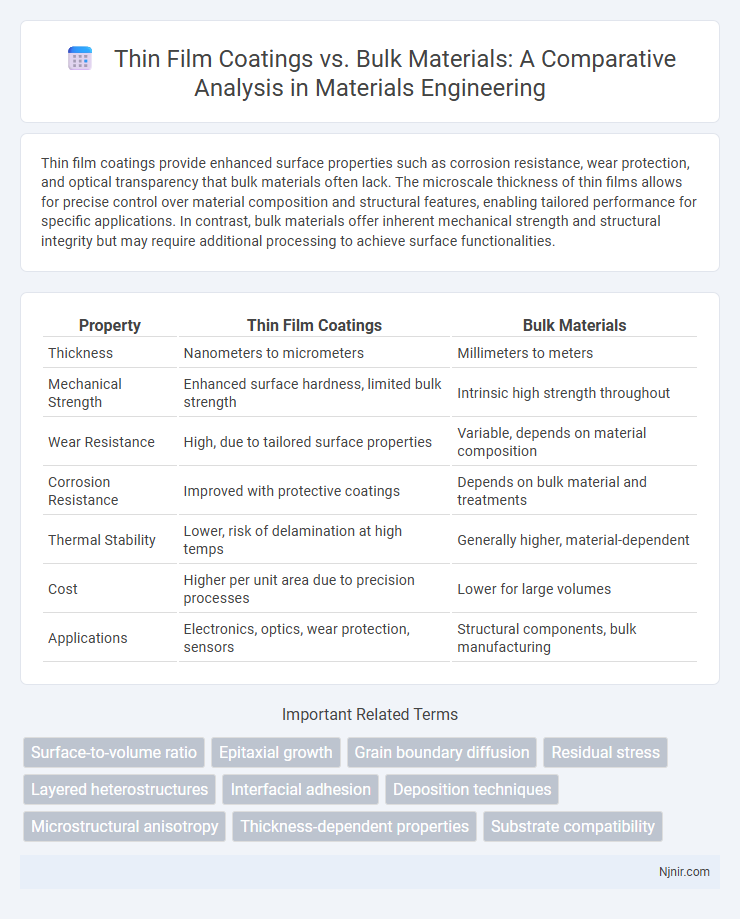
Table of Comparison
| Property | Thin Film Coatings | Bulk Materials |
|---|---|---|
| Thickness | Nanometers to micrometers | Millimeters to meters |
| Mechanical Strength | Enhanced surface hardness, limited bulk strength | Intrinsic high strength throughout |
| Wear Resistance | High, due to tailored surface properties | Variable, depends on material composition |
| Corrosion Resistance | Improved with protective coatings | Depends on bulk material and treatments |
| Thermal Stability | Lower, risk of delamination at high temps | Generally higher, material-dependent |
| Cost | Higher per unit area due to precision processes | Lower for large volumes |
| Applications | Electronics, optics, wear protection, sensors | Structural components, bulk manufacturing |
Introduction to Thin Film Coatings and Bulk Materials
Thin film coatings are ultra-thin layers of material deposited on substrates to enhance surface properties such as hardness, corrosion resistance, and optical performance, typically ranging from a few nanometers to micrometers in thickness. Bulk materials consist of homogeneous, thick solid volumes that exhibit intrinsic mechanical, thermal, and electrical properties independent of surface modifications. Understanding the distinct structural dimensions and functional advantages of thin film coatings versus bulk materials is essential for applications in electronics, optics, and protective surfaces.
Material Properties: Thin Films vs Bulk Forms
Thin film coatings exhibit distinct material properties compared to their bulk counterparts, such as enhanced hardness, improved wear resistance, and altered optical characteristics due to their nanoscale thickness and microstructure. These coatings often demonstrate higher surface energy and altered electrical conductivity, influenced by grain size, residual stress, and substrate interactions, which are less pronounced in bulk materials. The unique mechanical and chemical behavior of thin films arises from their reduced dimensionality and interface effects, enabling tailored performance in applications like electronics, optics, and protective layers.
Fabrication Techniques: Coatings and Bulk Production
Thin film coatings are typically fabricated using physical vapor deposition (PVD), chemical vapor deposition (CVD), or atomic layer deposition (ALD) techniques, which enable precise control over thickness and composition at the nanoscale. Bulk materials, in contrast, are produced through casting, forging, extrusion, and powder metallurgy, processes designed to shape and consolidate materials at macroscopic scales while ensuring mechanical integrity. Advanced fabrication methods for thin films enhance surface properties such as wear resistance and corrosion protection, whereas bulk production focuses on optimizing the overall material structure and performance.
Mechanical Behavior Comparison
Thin film coatings exhibit higher hardness and increased wear resistance compared to bulk materials due to their constrained microstructure and grain size refinement. The mechanical behavior of thin films is dominated by surface effects, leading to enhanced elastic modulus and yield strength, whereas bulk materials display uniform deformation governed by their inherent crystalline structure. Delamination and residual stress accumulation are critical challenges in thin films that significantly affect their mechanical performance, contrasting with the more predictable fracture toughness and ductility of bulk substrates.
Surface Engineering and Functionalization
Thin film coatings enhance surface engineering by providing precise control over material properties such as hardness, corrosion resistance, and optical characteristics without altering the bulk structure. These coatings enable functionalization at the nanoscale, improving wear resistance, chemical activity, and biocompatibility compared to bulk materials. Surface modification via thin films allows tailored interfaces crucial for applications in electronics, aerospace, and biomedical devices.
Applications in Modern Industries
Thin film coatings enhance the surface properties of bulk materials by providing improved hardness, corrosion resistance, and optical characteristics critical in modern industries such as electronics, aerospace, and medical devices. These coatings enable precise control over electrical conductivity and thermal insulation, essential for semiconductor manufacturing and energy-efficient solar panels. Bulk materials offer structural integrity, while thin films customize functional surfaces, creating hybrid solutions that optimize performance and durability in advanced technological applications.
Environmental Stability and Durability
Thin film coatings exhibit enhanced environmental stability by providing protective barriers against moisture, UV radiation, and chemical corrosion, significantly extending the lifespan of underlying bulk materials. These coatings offer superior durability through resistance to abrasion, scratches, and thermal cycling compared to uncoated bulk substrates. The integration of thin films improves mechanical strength and reduces degradation rates, making them ideal for harsh environmental conditions.
Cost and Resource Considerations
Thin film coatings offer significant cost savings compared to bulk materials by using minimal substrate material while providing enhanced surface properties such as corrosion resistance and wear protection. Resource efficiency is improved as thin films require less raw material and energy during deposition, reducing overall manufacturing expenses and environmental impact. Bulk materials demand higher raw material volumes and machining costs, making thin films a more economical choice for optimizing material performance and resource utilization.
Advancements in Characterization Methods
Advancements in characterization methods for thin film coatings versus bulk materials have significantly enhanced the precision and depth of material analysis. Techniques such as atomic force microscopy (AFM), X-ray photoelectron spectroscopy (XPS), and time-of-flight secondary ion mass spectrometry (TOF-SIMS) provide nanoscale surface morphology, chemical composition, and depth profiling critical for thin films. In contrast, bulk material analysis benefits from improved X-ray diffraction (XRD) and electron backscatter diffraction (EBSD), enabling detailed crystallographic and microstructural investigations essential for performance optimization.
Future Trends in Materials Selection
Future trends in materials selection emphasize the integration of thin film coatings with bulk materials to enhance performance characteristics such as corrosion resistance, wear resistance, and thermal stability. Advanced deposition techniques like atomic layer deposition (ALD) and chemical vapor deposition (CVD) enable precise control over thin film thickness and composition, optimizing functionality for industries ranging from electronics to aerospace. Ongoing research focuses on developing multifunctional coatings that provide tailored mechanical, electrical, and optical properties while maintaining the bulk material's structural integrity.
Surface-to-volume ratio
Thin film coatings exhibit a significantly higher surface-to-volume ratio than bulk materials, enhancing their reactivity, catalytic efficiency, and surface-specific properties.
Epitaxial growth
Epitaxial growth enables precisely controlled thin film coatings with superior crystalline quality compared to bulk materials, enhancing electronic and optical device performance.
Grain boundary diffusion
Grain boundary diffusion in thin film coatings significantly enhances atomic transport compared to bulk materials due to their higher grain boundary density and reduced grain size.
Residual stress
Thin film coatings exhibit significantly higher residual stress compared to bulk materials due to their constrained microstructure and deposition conditions, impacting mechanical performance and reliability.
Layered heterostructures
Layered heterostructures in thin film coatings provide enhanced mechanical, optical, and electronic properties compared to bulk materials by enabling precise control over thickness, composition, and interface quality.
Interfacial adhesion
Thin film coatings exhibit superior interfacial adhesion compared to bulk materials due to their enhanced surface bonding mechanisms and reduced stress concentrations at the interface.
Deposition techniques
Thin film coatings utilize advanced deposition techniques such as chemical vapor deposition (CVD), physical vapor deposition (PVD), and atomic layer deposition (ALD) to achieve controlled thickness and surface properties, whereas bulk materials are typically processed through casting, forging, or machining without specialized thin-layer deposition methods.
Microstructural anisotropy
Thin film coatings exhibit pronounced microstructural anisotropy compared to bulk materials, resulting in unique mechanical, optical, and electrical properties tailored by their layered atomic arrangements.
Thickness-dependent properties
Thin film coatings exhibit thickness-dependent properties such as enhanced optical transparency, increased hardness, and altered electrical conductivity compared to bulk materials due to quantum confinement and surface-to-volume ratio effects.
Substrate compatibility
Thin film coatings enhance substrate compatibility by providing tailored surface properties without altering the bulk material's structural integrity.
Thin Film Coatings vs Bulk Materials Infographic